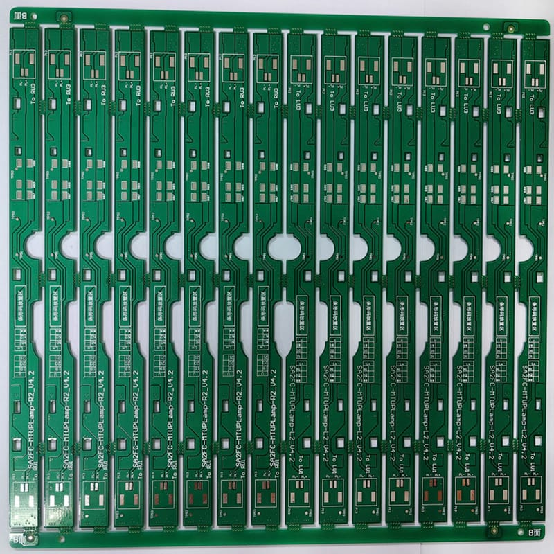
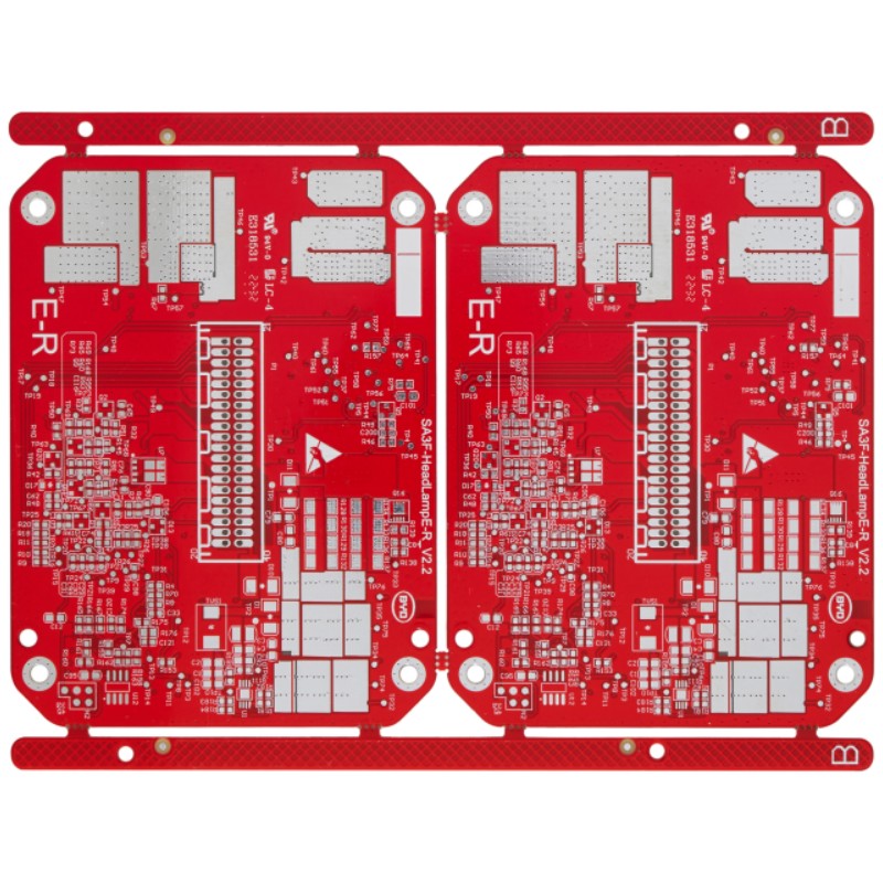
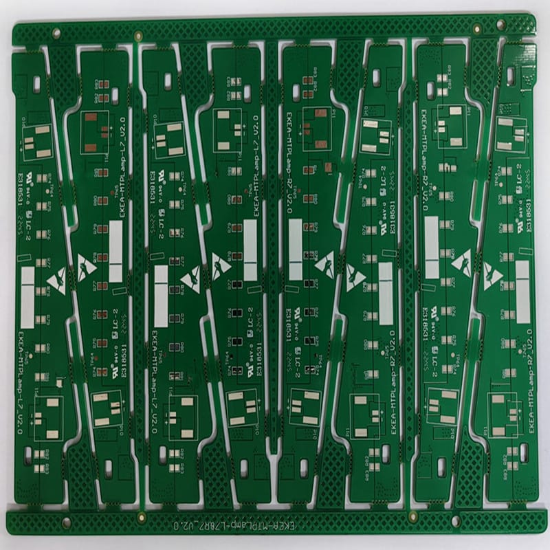
Prototype printed circuit boards RED solder mask castellated holes
Prototype printed circuit boards RED solder mask castellated holes
Looking for prototype PCBs with RED solder mask and castellated holes? Look no further! We are a factory specializing in manufacturing high-quality PCBs.
The processes of plated half holes are: 1. Process the half-side hole with double V-shaped cutting tool.2. The second drill adds guide holes on the side of the hole, removes the copper skin in advance, reduces burrs, and uses groove cutters instead of drills to optimize the speed and drop speed.3. Immerse copper to electroplate the substrate, so that a layer of copper is electroplated on the hole wall of the round hole on the edge of the board.4. Production of the outer layer circuit after lamination, exposure, and development of the substrate in sequence, the substrate is subjected to secondary copper plating and tin plating, so that the copper layer on the hole wall of the round hole on the edge of the board is thickened and the copper layer is covered with covered by a tin layer for corrosion resistance;5. Half-hole forming cut the round hole on the edge of the board in half to form a half-hole;6. In the step of removing the film, the anti-electroplating film pressed during the film pressing process is removed;7. Etching the substrate is etched, and the exposed copper on the outer layer of the substrate is removed by etching;8. Tin stripping the substrate is stripped of tin, so that the tin on the half-hole wall can be removed, and the copper layer on the half-hole wall is exposed.9. After forming, use red tape to stick the unit boards together, and remove the burrs through the alkaline etching line10. After the second copper plating and tin plating on the substrate, the round hole on the edge of the board is cut in half to form a half hole, because the copper layer of the hole wall is covered with a tin layer, and the copper layer of the hole wall is completely intact with the copper layer of the outer layer of the substrate Connection, involving strong bonding force, can effectively prevent the copper layer on the hole wall from being pulled off or copper warping when cutting;11. After the half-hole forming is completed, the film is removed and then etched, so that the copper surface will not be oxidized, effectively avoiding the occurrence of residual copper or even short circuit, and improving the yield rate of the metallized half-hole PCB circuit board.